Journal of the Mexican Chemical Society, vol. 64, no. 2, 2020
Sociedad Química de México A.C.
Deeptimayee Khatua
Department of Chemistry, Siksha ‘O’ Anusandhan, Deemed to be University, Khandagiri Square, Bhubaneswar- 751030 India)., India
Sujit Kumar Dehury
P.G. Department of Chemistry, Vikram Deb (Autonomous) College, Jeypore.
S.K. Parida
Department of Physics, Siksha ‘O’ Anusandhan, Deemed to be University, Khandagiri Square, Bhubaneswar- 751030 India)., India
R. N. P. Choudhary
Department of Physics, Siksha ‘O’ Anusandhan, Deemed to be University, Khandagiri Square, Bhubaneswar- 751030 India)., India
P. Ganga Raju Achary *
Department of Chemistry, Siksha ‘O’ Anusandhan, Deemed to be University, Khandagiri Square, Bhubaneswar- 751030 India)., India
Received: 20 June 2019
Accepted: 14 January 2020
Funding
Funding source: UGC-DAE-CSR
Contract number: CRS-M-297
Abstract : A lead-based multiferroic, Pb(Co1/3Mn1/3W1/3)O3, was synthesized by using a high-temperature solid-state reaction technique. Based on X-ray structural analysis, an orthorhombic crystal structure has been suggested for the material. The scanning electron microscopy (SEM) image exhibits a morphology with and uniform grains distribution. A detailed study of variation of dielectric parameters with frequency and temperature exhibits that Pb(Co1/3Mn1/3W1/3)O3 undergoes multiple phase transitions; first transition (T c1 ) appeared at 436K (ferroelastic to ferroelectric) whereas second transition ( T c2 ) appeared at 504K ( ferroelectric to paraelectric). Since the peaks of dielectric constant are broader and diffused, a diffusivity parameter (γ) has been estimated to the amount of disordering in the material structure.The contribution of grain,grain boundaries and electrode effect in electrical conduction mechanisim can be understood by frequency-temperature dependence of resistive characterestics using CIS spectroscopy (complex impedance spectroscopy). Impedance or Nyquist plots were modeled with an equivalent circuit having capacitance, resistance and related parameters. Studies of transport properties, ac conductivity, electrical modulus and magneto-electric (ME) effect of the materialis reported in this communication.
Keywords: Multiferroic material, electrical properties, Nyquist plots, dielectric relaxation.
Resumen: Se sintetizó un Pb(Co1/3Mn1/3W1/3 )O3 multiferroico a base de plomo mediante una técnica de reacción en estado sólido a alta temperatura. Basado en el análisis estructural de rayos X, se ha sugerido una estructura de cristal ortorrómbica para el material. La imagen de microscopía electrónica de barrido (SEM) muestra una morfología con una distribución de granos casi similar y uniforme. El estudio detallado de la variación de los parámetros dieléctricos con frecuencia y temperatura demuestra que Pb(Co1/3Mn1/3W1/3)O3 experimenta múltiples transiciones de fase; la primera transición (T c1 ) apareció a 436K (ferroelástico a ferroeléctrico) mientras que la segunda transición (T c2 ) apareció a 504K (ferroeléctrico a paraeléctrico). Dado que los picos de la constante dieléctrica son más amplios y difusos, se ha estimado un parámetro de difusividad (γ) en función de la cantidad de desorden en la estructura del material. Dependencia de la temperatura de las características de resistencia mediante espectroscopia CIS (espectroscopia de impedancia compleja). Los diagramas de impedancia o Nyquist se modelaron con un circuito equivalente que tiene capacitancia, resistencia y parámetros relacionados. Los estudios de las propiedades de transporte, la conductividad de CA, el módulo eléctrico y el efecto magnetoeléctrico (ME) del material se informan en esta comunicació.
Palabras clave: Material multiferroico, propiedadeselectricas, parcelas de Nyquist, relajación dieléctrica.
Introduction
The selection of the word ‘multiferroics’ for a single- phase material was considered to have minimum of two ferroic properties. However, today the range of ‘multiferroic’ is broadened to include the materials having all types of magnetic ordering, unconstrained electric polarization, or potentially ferroelasticity [1]. The subject domain of the multiferroics was developed due to extensive research in the magnetoelectric systems. The multiferroics became the thrust area of current research which may be due to the development of the thin film of BiFeO3 in the year 2003 [2]. Subsequent research publications on the solid magnetic and electric coupling in orthorhombic TbMnO3 [3] and TbMn2O5 [4] have attracted much attention to research work on multiferroics. In addition to the above, some recent work on the Pb-based multiferroic materials, such Pb(Fe,W)O3, Pb(Co,W)O3, Pb(Mg,W)O3, Pb(Fe,Nb)O3, Pb(Co,W)O3 or binary solid solution (BiFeO3-Pb(ZrTi)O3), has been found useful because of their applications in electronic devices (i.e;transducer, filter and resonator, actuator, ultrasonic motor/vibrator,piezoelectric transformer, computer memory etc. [5,6] Further, the high-temperature (~1200oC)processing (calcination/sintering) of such type of materials is a matter of a great concern, as the ingredients like PbO are volatile at high temperature causing compositional variation and creation of defects in the final products. The excess energy consumption for the fabrication of these materials also addsto the cost of the end product. In order to make the fabrication of the materials cost effective and less time consuming process, numerous processing methods were suggested including chemical processing methods,solid phase calcination ,sintering, processes at low temperatures [7]. Although all the methods were scientific, low-temperaure calcination/sintering processing of the materials becomes popular for multiple reasons [8,9]. In the initial stages of solid state reaction, a eutectic composition may take place. As a result, the sintering temperature of some ferroelectrics or multiferroic ceramics could be significantly decreased by selecting asuitable processing route. From the detailed literature survey it is found that many lead-based complexes were synthesized using various technique such as Pb(B´B″)O3; Pb(Fe0.5Ta0.5)O3(PFT), Pb(Zr1-x,Tix)O3(PZT)(0<x<1), 0.8Pb(Fe0.33W0.67)O3-0.2PbTiO3, (1-x)Pb(Fe0.5Nb0.5)O3(PFN)-xPb(Zr0.2Ti0.8)O3, Pb(Fe0.5Nb0.5)O3-Pb(Zn1/3Nb2/3)O3,0.65[Pb(Ni1/3Nb2/3)O3]-0.35PbTiO3, etc. [10] using a solid phase sintering at high temperatures. In view of the importance of the materials and with the main objectives to prepare low cost suitable lead - based multiferroic materials at low temperatures to provide high value of dielectric constant, low value of tangent loss, and other related suitable parameters useful for devices, we have prepared Pb(Co1/3Mn1/3W1/3)O3 (PCMW) and studied its microstructural, capacitive and resistive and magnetoelectric chararacterstics which are reported in this paper. A perovskite compound having their ferroelectric and magnetic ions in the octahedral position, show both the electric and magnetic ordering simultaneously. Hence, in this paper the Mn+2and W+6ions both were introduced at the B-site which serve as ferroelectric and magnetic ions respectively with Pb+2 ions at the A site [11].
Experimental
The perovskite material PCMW was synthesized by using high-purity oxides; PbO, CoO, MnO2 and WO3 through a cost-effective solid-state reaction route. These precursors were weighed according to their molar ratios. Then the mix powder was ground manually for 2 to 3h in an agate mortar and pestle to form the desired material, Pb(Co1/3Mn1/3W1/3)O3. Finally, it was mixed in presence of ethanol for 2h. The mixed powder was transferred to the aluminium crucible, then it was subjected to the muffle furnace at 1073K for 4 h for calcinations.After the calcination the material, it was further ground again till it became fine powder. The diffractogram of the fine powder was taken to obtain X-ray diffraction data using Rigaku X-ray diffractometer with λ=1.5405 Å having 2θ value 200 to 800 to check the phase formation of the material. The pellets of PCMW were prepared of dimension 10mm diameter and thickness around 2 mm and placed in the high-temperature furnace again on a clean alumina boat for sintering at 11300C for 10 h. Then, the PCMW pellets were cooled to 298 K (1 day) to avoid any type thermal shock. The sintered pellets were taken from the oven and verified its texture and breakage to ensure proper sintering of the pellet. One such properly sintered pellet is gold coated and set for the morphology study using a SEM apparatus having model JEOL-JSM-6400 at 20kV. The second pellet was made conducting both sides by applying uniform Ag-paint (high conducting) and put it in a hot air oven at 410K (2h) to check the removal of moisture or impurities(volatile). The electroding on the faces of the pellet was also checked before the electrical and dielectric analysis of PCMW using the LCR (impedance analyser or phase-sensitive meter (PSM)). The various electrical parameters were measured in the temperatures range of 300 K to 600 K and frequency range of 100Hz to 1MHz.
Results and discussion
Structural and microstructural analysis
The XRD patterns of synthesized PCMW, analyzed by rigakuultima iv x-raydiffractometer with CuKα radiation where λ = 1.54056 Å and 10° ≤ 2θ ≤ 80° which is depicted in Fig. 1(a). The peaks corresponding to 2Ө values 27.541°,45.348° and 29.10° are due to the impurity phase lead tungstate. The Rietveld refinement profiles of PCMW was shown in Fig 1(c) . The refinement of the crystal structure of the material has been accomplished by GSAS-II software. Pb2MnWO6 withan orthorhombic crystal system (space group Pmc211) is taken as reference model from crystallography open database (COD)[12].The initial values of cell parameters are a= 11.640 b=8.0198 c=5.780 . It can be clearly observed in Fig. 1(c) that the peaks and the intensities of the present sample are perfectly matched with the model. The Rietvield refinement pattern confirms the Orthorhombic structure (space group- Pmc211) of PCMW sample and the refined structural parameters are found to be a=11.64026, b=8.00857, c=5.81662Å with Rwless than10%. Fig. 1(b) depicts the SEM micrograph of the surface of the pellet of PCMW. It illustrates similar nature of grains with a size variation of 1.5 to 5.0 µm. The Dhkl(average crystallite size)of PCMW was found to be49.99nm, which was obtained by using Scherrer’s equation,i.e; D hkl =Kλ/ β 0.5 Cos θ where K is constant (= 0.89), λ= 1.541Å, and β 0.5 is FWHM i.e; fullwidth at half maximum[13]. Fig 1(d) depicts the energy dispersive spectra of PCMW sample. This figure confirms the presence of all the elements in the stotchiometric ratio (wt%) of the sample PCMW.
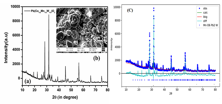
Fig. 1
XRD pattern (a) and typical SEM micrograph as inset (b) of Pb(Co1/3 Mn1/3 W1/3)O3 (c) Rietvield refined pattern of PCMW sample.
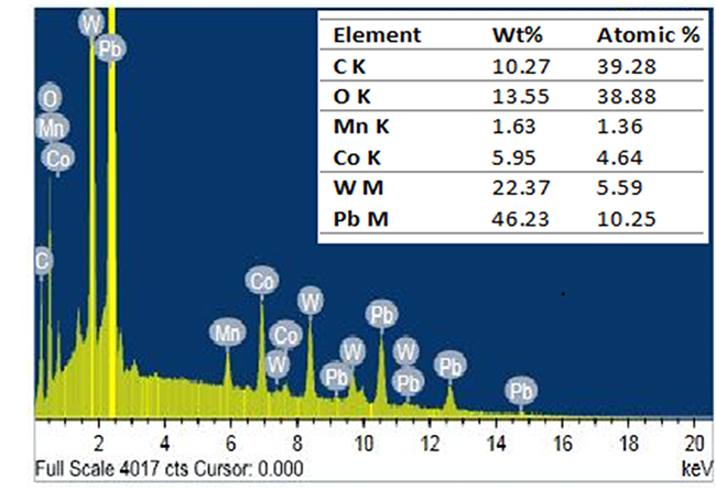
Fig. 1
(d) EDX analysis of PCMW sample.
Dielectric study
The frequency dependencce of the relative dielectric constant (ɛr) and dielecric loss (tan δ) of PCMW was shown in Fig 2. The ɛ r decreases from a high value at low frequency with the gradual decrease in frequency. This is due to the fact that the dispersion decreases with the increase in frequency. Also, the different types of polarizations, like dipolar, interfacial, ionic, atomic and electronic determine such a behaviour in the PCMW material.
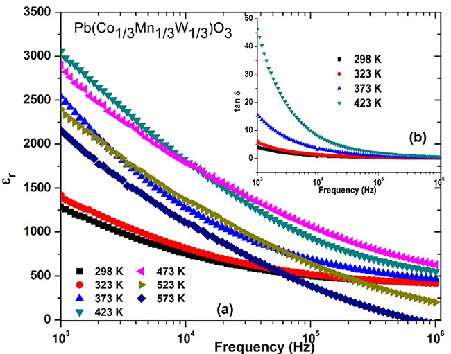
Fig. 2
(a)Frequency dependence of relative dielectric constant (ɛr) and (b) frequency dependence of loss tangent of Pb(Co1/3Mn1/3W1/3)O3.
In the high- frequency region, the dipoles are not aligned with the applied electric field when the frequency exceeds the certain limit, electronic polarization dominates over the dielectric constant. The value of dielectric loss follows the similar trend as of dielectric constant. This phenomenon is described by the two-layer model of Maxwell and Wagner [14,15]. According to the Maxwell and Wagner model, this behavior of the PCMW system is due to two layers, i.e, the conducting grains and less conducting grain boundaries of PCMW. At low frequencies, the activity of electron at grain boundaries increases though out the electrical conduction, whereas at higher frequency, the activity of electron is more at grains. Because at alow-frequency, the grain boundaries exhibit more resistance which is required high energy for charge transfer. Hence, at the low frequency both the the insulating parameter (ɛr and tan δ) exhibits higher value. The magnitude of these parameters decreases because it requires less energy for the motion of the charge carrier sat higher frequency region.
Fig. 3(a) represents temperature vs dielectric constant graph of the sample PCMW at 103 Hz,105 Hz and 106 Hz. The plot indicates that ɛ r gradually increases with arise in temperature, passes through one or two maxima and then decreases. At 103 Hz, ɛr increases from 742 at 298 K to its first maximum 1852 at 436 K, then it decreases and gives second maxima at 504 K with ɛr being 1812. Hence two peaks are obtained in the above plot( Fig. 3(a)).Also, the height of the plot (ɛꞌvs T) decreases with increasing frequency and such typical behaviour is referedas a relaxor ferro- or antiferroelectric material[16]. One peak basically disappears with increasing frequency, which is the typical relaxor-ferroelectric behavior. PbMnO3with P4/mmm space group is an anifferromagnetic material having TN approx. equal to 400 K [17]. The ferroelectric relaxor characteristics induces by the incorporation of Co or W at the B site of the perovskite. Furthermore, the data presented is in fact like a typical for ferroelectric transitions, which often occur in two steps, e.g. from paraelectric to ferroelectric to relaxor ferroelectric. The increase in dielectric permittivity is too large to be associated with a magnetic transition. The two peaks clearly look like two ferroelectric transitions.
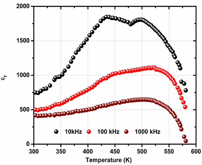
Fig. 3
(a)Temperature dependence of dielectric permittivity (ɛꞌ) at 10 kHz, 100 kHz and 1000 kHz of PCMW.
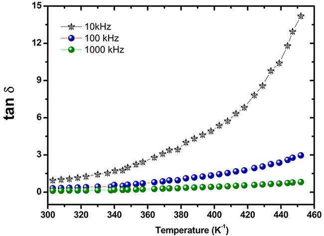
Fig. 3
(b) Temperature dependence of dielectric loss at 10 kHz, 100 kHz and 1000 kHz of PCMW.
The temperature, at which two maxima occur at 436 K and 504 K, are referred as the transition temperatures T c1 and T c2 respectively (Fig. 3(a)). This type of unique behaviour of the dielectric material justifies the existence of two phase transitions: (i) magnetic transition (Tc) at 436K and (ii) ferroelectric to paraelectric (Tc) at 504K[18].
However, inspecting Fig. 3(a) at frequencies 100 kHz and 1000 kHz, value of ɛ
r
is found to be smaller than that obtained at 10 kHz. First maxima (Tc) at 10 kHz becomes diffused, and appears as if it vanished. But, at higher frequencies, ɛ
r
gradually increases with an increase in temperature. At 298 K, the value of ɛ
r
is 499 and 418 at 100 and 1000 kHz respectively. As temperature increases, ɛr also increases, and reaches to a maxima 1115 (at 523 K) and 648(511 K). As dielectric (ɛ
r
) peaks are broadened or diffused in the high- frequency range, ‘diffusivity’ (γ) parameter (used as a measure of diffuse phase transition) in the ferroelectric material is calculated. Linear plot of  vs ln(T-T
c
) (Fig. 4) gives the value of diffusivity[19]. γ value is found to be 1.97 and 1.04 at 10 kHz and 100 kHz respectively. These values of γ lying between 2 and 1) clearly indicates the occurrence of phase transition of diffuse-type in the studied sample.
vs ln(T-T
c
) (Fig. 4) gives the value of diffusivity[19]. γ value is found to be 1.97 and 1.04 at 10 kHz and 100 kHz respectively. These values of γ lying between 2 and 1) clearly indicates the occurrence of phase transition of diffuse-type in the studied sample.
Fig 3 (b) shows the tan δ vs temperature graph of the sample. At room temperature (298 K), magnitude of tan δ at 10 kHz, 100 kHz and 1000 kHz are found to be 0.96, 0.31 and 0.11 respectively. The low value of tan δ could be maintained initially, for example, up to the first transition temperature (Tc) (Fig. 3(a)), the value of this parameter is 9.79, 2.25 and 0.66 at 104 Hz, 105 Hz and 106 Hz respectively. At low temperature the value of tangent loss increases and above the critical temperature it increases rapidly. The magnitude of tan δ increases in at higher temperature due to the following reasons: (i) the scattering of charge carriers (thermally activated), (ii) ferroelectric material having intrinsic defect and (iii) create oxygen ion vacancies due to high-temperature sintering of ferroelectric material and (iv) dominance of conductivity.
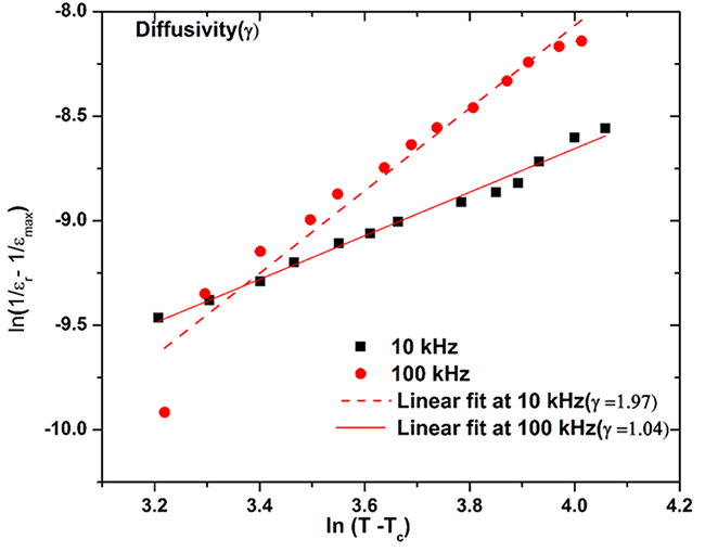
Fig. 4
Diffusivity(γ) plot of Pb(Co1/3Mn1/3W1/3)O3.
Complex impedance spectral analysis
A nondestructive CIS technique is used for find the electrical behaviour of ionic conductors, ferroelectric material and other ceramics. This technique is also useful to determine the benefacation of grains grain boundaries and electrode in the present material. Many important information can be obtained by comparing complex impendance and related electrical parameters.
Variation of Z′ with frequency at temperatures at 343K, 423K, 473K, 523K, 573K (with inset at 298K and 323K) is illustrated in Fig. 5 (a). With increasing frequency and temperature, the magnitude of Z′ decreases. The decrease in the magnitude of Z′ indicates that the present material becomes more conducting. So PCMW is behaving like a semiconductor with NTCR (negative temperature coefficient of resistance) behaviour. At higher frequency region i.e,>102 kHz the curves are merged at every temperature because of the barrier properties of the sample decrease due to the release of space charge[20]. The effect of frequency on imaginary impedance (Z′′) at different temperatures of PCMW is depicted in Fig. 5 (b). With the increase in temperature the peaks are shifted towards higher frequency region. Similarly the real impedance (Z′) vs frequency merge at high frequencies at various temperatures, which describes the temperature dependence of the relaxation process[14][21]. Fig. 5 (b) describes the presence of multiple relaxation time due to the small broadening of the peaks. At higher temperature relaxation is due to the presence of oxygen vacancies whereas at low frequency it is for electron mobility. The hopping mechanisim of the electrons, oxygen ion vacancies and defects on the material plays an important role in electrical conduction in PCMW.
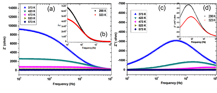
Fig. 5
(a) Frequencydependence of Z′(373 K to 573 K, (b) frequency vs Z′ (inset ) at (298K and 323 K), (c) Frequency dependence of Z′′ (373 K to 573 K and (d) frequency vs Z′′ (inset) at (298K and 323 K) of Pb(Co1/3Mn1/3W1/3)O3.
Fig. 6 shows the Nyquist plots at various temperatures in a wide frequency range (1kHz to 1MHz). Semicircular arcs which are formed in the Nyquist plot, describes the role of grain, electrode or interface effects in the resistive and capacitive behaviours of the PCMW material. Fig. 6 (inset) represents an equivalent CQR for low temperatures and {(CQR) (CR)} circuit for high temperatures, which describes the above effect. where C and Q are A(jω)m-1 and A(jω)n-1respectivly and A is Jonscher’s universal components [22,23]. The above circuit has been designed by using the software ZSIMP WIN version 2. Fig. 6 clearly indicates the presence of one symmetric semicircle having center lying on the Z′ axis. This implies that only one dielectric contribution is present. This may well be the intrinsic bulk dielectric contribution and no signs of any Maxwell-Wagner relaxation or grain boundary contribution are evident. The perfect arcs on the graph (Fig. 6) confirm the well preparation of PCMW material. Where the non- Debye-type of relaxation was calculated by establishment of a CPE (constant phase element) with parallel RC network. The value Y (admittance) of CPE can be calculated by using the formulaYCPE = A0(jω)n = Aωn+ jBωn, where A = A 0 Cos(nπ/2) and B = A 0 Sin(nπ/2) [22]. Where A0 (the measure of the dispersion)and n are being frequency independent but temperature dependent parameters .The value of n lies between 0 (for ideal resistor) and 1(for ideal capacitor)[24]. The model fitted bulk resistance(Rb)and grain boundary resistance (Rgb) give the NTCR behaviour of the PCMW sample [25].
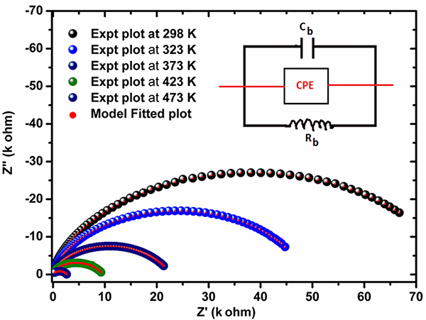
Fig. 6
The Nyquist plots Pb(Co1/3Mn1/3W1/3)O3 with an equivalent circuit of (CQR) at different temperatures.
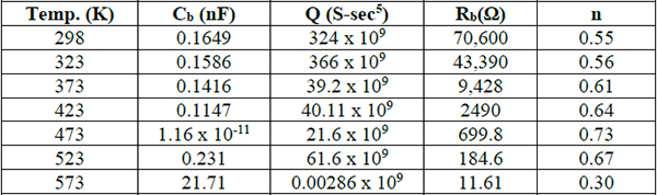
Table 1 lists the estimated parameters such as bulk (grain) and grain boundary resistance and capacitance, at given temperatures. The value of bulk resistance (R b ) decreases from 70,600 Ohm at 298 K to 11.61 Ohm at 573K shows the semiconducting nature of the material with increase in temperature the PCMW behaves as conductor due to the decrease in bulk capacitance.
Fitteted circuit parameters of grain /grain boundary resistance/ capacitance at various temperature.
Electrical conductivity
The effect of frequency on AC conductivity (σAC) is shown in Fig. 7(a). The magnitude of σAC of the PCMW material was calculated by using the formula σ AC = ωϵ r ϵ o tanδ. The variation of σ ac with inverse of absolute temperature (10 3 /T) at various frequency ranges is reported in Fig 7 (b). Activation energy (E a ) of the material was calculated from the slope of the plot by using the equation σ = σ o exp (-E a /K B T), where σ o = pre-exponential factor and K B =Boltzmann constant. At low temperature, E a is found to be 0.695, 0.687 and 0.773 at 104 Hz, 105 Hz and 106 Hz respectively. The activation energy of the sample is gretter than 0.2 eV ,which supports the conduction mechanism due to the hopping of charge carriers[25][26][25]. The parts of ac conductivity curve could be completely described with Jonscher’s power law :σ t = σ dc + B σ ω n where the symbols have their usual meaning [21][20]; B is a constant. Both figures confirm that the PCMW material is semi-conducting in nature.
It is clearly observed from Fig. 7 (b) that at low-frequency region the value of activation energy is high but at high frequency region the value decreases because at lower frequency region the charge carriers move long distance which is responsible for conductivity and it require less energy[27][28].
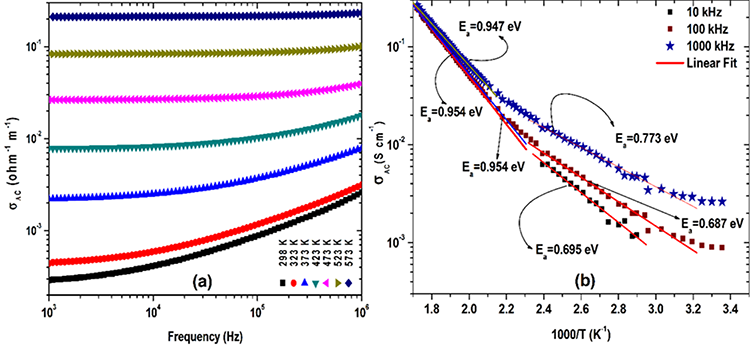
Fig. 7
(a) Frequency dependent AC conductivity (σac), (b) σacvs 1000/T of Pb(Co1/3Mn1/3W1/3)O3.
Electrical modulus
The information regarding interfacial polarisation time of relaxtation suppression electrode effect and ac conductivity of the sample can be analysed from the electrical modulus data which is a function of both frequency and temperature. By using the following equation the magnitude of the real (M’) and imaginary (M’’) modulus can be evaluated:
Fig. 8(a) and 8(b) illustare the real modulus (M′) and the imaginary modulus (M′′) vs frequency graph respectively. At low frequency region the value of real modulus tends to zero at different temperature due to the conduction of the charge carriers for short range and the the lack of restoring-force to travel the charge in an electric field environment[24]. With increase in frequency the value of M′ increases, and the value decreases with further increase in temperature. The imaginary part of the material similar trend and passes through a maximum wit increase in the frequency. By enhancing the temperature in the low frequency domain, the imaginary modulus M′′ decreases, but from 298K to 573K temperature the value of M′′ peaks moves towards right i.e; higher frequency region. The the Debye type behaviour of the material was confirmed from the symmetrical nature of the modulus plot.
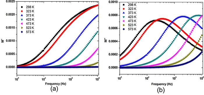
Fig. 8
Frequency dependence of M′ (a) and (b) frequency dependence of M′′ of Pb(Co1/3Mn1/3W1/3)O3.
Magneto-electric Study
The ME effect in a material is due to the presence of both magnetic and electric ordering. Both single phase and composite materials show the Magneto-electric effect. The present PCMW material is a single phase material.It shows M-E coupling due to the interaction between the magnetic and ferroelectric sub lattices, however in case of a composite the coupling is developed because of the interaction of piezoelectric and piezo-magnetic phases [24][13]. The ME voltage coefficient can be calculated by
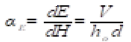 where E the induced electric field, H applied magnetic field, V ME voltage, h0 magnitude of the AC magnetic field and d thickness of the sample [29]. The field dependent magneto-electric voltage coefficient of PCMW is shown in the Fig. 9.
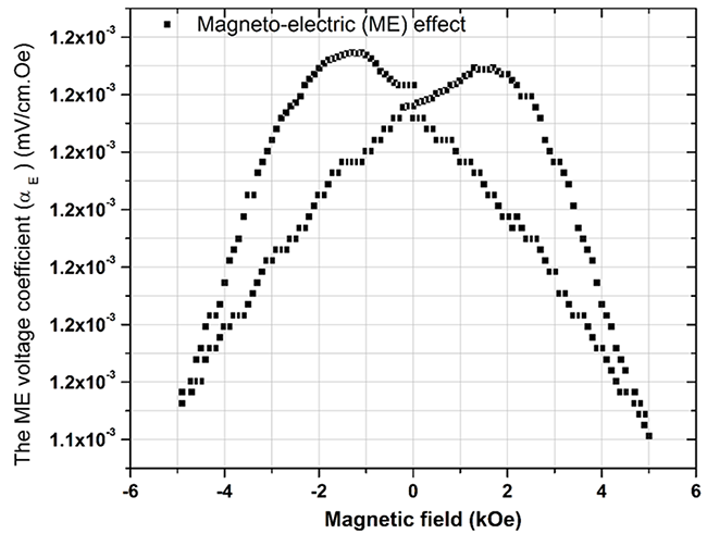
Fig. 9
Room temperature magnetic field dependence of ME voltage coefficient of Pb(Co1/3Mn1/3W1/3)O3.
Conclusion
In summary, a single phase Multiferroic Perovskite Pb(Co1/3Mn1/3W1/3)O3 was synthesized successfully by using cost effective solid-state reaction route. The X-ray diffraction analysis confirms the orthorhombic phase of the system. The SEM image confirms the grains were uniformly distributed throughout the surface of the PCMW sample. Pb(Co1/3Mn1/3W1/3)O3 experimental dielectric data reveals a typical behavior of ferroelectric transitions, which often occur in two steps, e.g. from paraelectric to ferroelectric to relaxor ferroelectric. The charge carriers were followed the hopping mechanisim hence the sample undergoes thermally activated relaxation process. It shows two phase transitions; the first transition Tc appeared at 436K ( magnetic) and the second transition Tc appeared at 504K ( ferroelectric to paraelectric) which is confirmed from the dielectric constant vs temperature plot. The doping or incorporation of Co or W at the B site of the pervoskite induces the ferroelectric relaxor characterstics. The relaxor properties of the the presented Pb(Co1/3Mn1/3W1/3)O3 can be tuned with the doping of Co/or W to design promising relaxor ferroelectric.
Acknowledgments
The present work is funded by the UGC-DAE-CSR, Mumbai (CRS-M-297) the author Dr.P.G.R. Achary is the reciepent of the grant.
References
1. Ascher, E.; Rieder, H.; Schmid, H.; Stössel, H. J. Appl. Phys. 1966, 37, 1404. DOI: https://doi.org/10.1063/1.1708493.
2. Wang, J.; Neaton, J.B.; Zheng, H.; Nagarajan, V.; Ogale, S.B.; Liu, B.; Viehland, D.; Vaithyanathan, V.; Schlom, Waghmare, U.V.; Spaldin, N.A.; Rabe, K.M.; Wuttig, M.; Ramesh, R. Science 2003, 299,1719. DOI: https://doi.org/10.1126/science.1080615.
3. Kimura, T.; Goto, T.; Shintani, H.; Ishizaka, K.; Arima, T.; Tokura, Y. Nature 2003, 426, 55. DOI: https://doi.org/10.1038/nature02018.
4. Hur, N.; Park, S.; Sharma, P.A.; Ahn, J.S.; Guha, S.; Cheong, S-W Nature 2004, 429, 392. DOI: https://doi.org/10.1038/nature02572.
5. Yoo, J.; Yoon, K.; Lee, Y.; Suh, S.; Kim, J.; Yoo, C. Jpn. J. Appl. Phys. 2000, 39, 2680. DOI: https://doi.org/10.1143/JJAP.39.2680.
6. Sasaki, Y.; Yamamoto, M.; Ochi, A.; Inoue, T.; Takahashi, S. Jpn. J. Appl. Phys. 1999, 38, 5598. DOI: https://doi.org/10.1143/JJAP.38.5598.
7. Masao, K.; Kazuaki, K. J. Am. Ceram. Soc. 2004, 84, 2469-2474.DOI: https://doi.org/10.1111/j.1151-2916.2001.tb01037.x.
8. Corker, D. L.; Whatmore, R. W.; Ringgaard, E.; Wolny, W. W. J. Eur. Ceram. Soc. 2000, 20, 2039-2045. DOI: https://doi.org/https://doi.org/10.1016/S09552219(00)00089-3.
9. Hayashi, T.; Hasegawa, T.; Tomizawa, J.; Akiyama, Y. Jpn. J. Appl. Phys. 2003, 42, 6074. DOI: https://doi.org/10.1143/JJAP.42.6074/meta.
10. Sanchez, D. A.; Ortega, N.; Kumar, A.; Roque-Malherbe, R.; Polanco, R.; Scott, J. F.; Katiyar, R. S. AIP Adv. 2011, 1, 42169. DOI: https://doi.org/10.1063/1.3670361.
11. Mathe, V. L.; Patankar, K. K.; Lotke, S. D.; Joshi, P. B.; Patil, S. A. Bull. Mater. Sci. 2002, 25, 347-350. DOI: https://doi.org/10.1007/BF02704130.
12. Quirós, M.; Gražulis, S.; Girdzijauskait\.e, S. .; Merkys, A.; Vaitkus, A. J. Cheminform. 2018, 10. DOI: https://doi.org/10.1186/s13321-018-0279-6.
13. Vasconcelos, D. C. L.; Costa, V. C.; Nunes, E. H. M.; Sabioni, A. C. S.; Gasparon, M.; Vasconcelos, W. L. Mater. Sci. Appl. 2011, 02, 1375-1382. DOI: https://doi.org/10.4236/msa.2011.210186.
14. Koops, C. G. Phys. Rev. 1951, 83, 121-124. DOI: https://doi.org/10.1103/PhysRev.83.121 .
15. Pawar, R. P.; Puri, V. Ceram. Int. 2014, 40, 10423-10430. DOI: https://doi.org/http://dx.doi.org/10.1016/j.ceramint.2014.03.013.
16. Dos santos-García, A. J.; Solana-Madruga, E.; Ritter, C.; Andrada-Chacón, A.; Sánchez-Benítez, J.; Mompean, F. J.; Garcia-Hernandez, M.; Sáez-Puche, R.; Schmidt, R. Angew. Chemie Int. Ed. 2017, 56, 4438-4442. DOI: https://doi.org/10.1002/anie.201609762.
17. Goodenough, J. B.; Zhou, J. Sci. Technol. Adv. Mater. 2015, 16, 36003. DOI: https://doi.org/10.1088/1468-6996/16/3/036003.
18. Liang, F.; Hui, Z.; Bolin, W.; Runzhang, Y. Prog. Cryst. Growth Charact. Mater. 2000, 40, 161-165. DOI: https://doi.org/10.1016/S0960-8974(00)00037-1.
19. Pilgrim, S. M.; Sutherland, A. E.; Winzer, S. R. J. Am. Ceram. Soc. 1990, 73, 3122-3125. DOI: https://doi.org/10.1111/j.1151-2916.1990.tb06733.x.
20. Kumar, A.; Singh, B. P.; Choudhary, R. N. P.; Thakur, A. K. J. Alloys Compd. 2005, 394, 292-302. DOI: https://doi.org/http://dx.doi.org/10.1016/j.jallcom.2004.11.012.
21. Ram, M. J. Alloys Compd. 2011, 509, 1744-1748. DOI: https://doi.org/http://dx.doi.org/10.1016/j.jallcom.2010.09.212.
22. Jonscher, A. K. J. Phys. D. Appl. Phys. 1999, 32, R57. DOI: https://doi.org/10.1088/0022-3727/32/14/201.
23. Jonscher, A. K. Nature 1977, 267, 673-679. DOI: https://doi.org/10.1038/267673a0.
24. Ross Macdonald, J. Solid State Ionics 1984, 13, 147-149. DOI: https://doi.org/http://dx.doi.org/10.1016/0167-2738(84)90049-3.}
25. Ranjan, R.; Kumar, R.; Kumar, N.; Behera, B.; Choudhary, R. N. P. J. Alloys Compd. 2011, 509, 6388-6394. DOI: https://doi.org/http://dx.doi.org/10.1016/j.jallcom.2011.03.003.
26. Sen, S.; Choudhary, R. N. P.; Pramanik, P. Phys. B Condens. Matter 2007, 387, 56-62. DOI: https://doi.org/http://dx.doi.org/10.1016/j.physb.2006.03.028.
27. Hirose, N.; West, A. R. J. Am. Ceram. Soc. 1996, 79, 1633-1641. DOI: https://doi.org/10.1111/j.1151-2916.1996.tb08775.x.
28. Gabal, M. A. E.-F.; Al Angari, Y. M.; Obaid, A. Y. Comptes Rendus Chim. 2013, 16, 704-711. DOI: https://doi.org/http://dx.doi.org/10.1016/j.crci.2013.01.009.
29. Shi, M.; Zuo, R.; Xu, Y.; Wang, L.; Gu, C.; Su, H.; Zhong, J.; Yu, G. Ceram. Int. 2014, 40 , 9249-9256. DOI: https://doi.org/http://dx.doi.org/10.1016/j.ceramint.2014.01.146.
Author notes
*Corresponding author: P. Ganga Raju Achary, Phone number: +91-8763124685, Fax Number: +91-6742351880, email: pgrachary@soa.ac.in
